By Ronald D. Schaeffer
Laser micromanufacturing is just like traditional manufacturing except that we use photons (light!) instead of, for instance, drill bits and saw blades. Lasers are used for machining, marking, welding and surface treatment. This article provides a brief summary of how lasers are used in several exemplary situations. In conclusion, a discussion is made concerning the use of Contract Manufacturers with respect to owning in-house laser tools. First though, it is important to define ‘micromanufacturing.’ Our definition of it is that the process involves lasers for material removal, addition or alteration and furthermore, the feature sizes on target are less than 1 mm (and usually much less) and the material thickness is also less than 1 mm (and again, usually much less).
Perhaps we should start with the definition of a laser. LASER (Light Amplified Stimulated Emission of Radiation) light has some unique properties that make it attractive for machining purposes. So, why use lasers for materials processing? First, they are non-contact meaning that there is less chance of damage to the part and no tool wear. Second, they can be very selective in the material removal or joining process. By choosing the right laser wavelength and energy density on target, we can, in many cases, remove one material selectively over another or weld dissimilar materials. A third reason is that lasers can be very flexible. We frequently encounter situations where high volume manufacturing of a part might be more affordable using custom, hard tooling, but this is very expensive and cannot usually be done for prototypes. Lasers make exceptional prototyping devices because of this flexibility. Finally, they can frequently replace other technologies that have their own inherent disadvantages.
Because lasers are available from the infrared portion of the electromagnetic spectrum through the ultraviolet, we have a lot of choices concerning just which laser to use. In general, IR lasers (like CO2 and Nd:YAG for instance) are infrared lasers and the material removal is by a first order thermal mechanism. UV lasers on the other hand can, in principle, have enough photon energy to break chemical bonds without heating the material and the first order removal mechanism is via a non-thermal or ‘cold’ process. Even for UV lasers though, longer pulse lengths can increase the thermal component of the laser processing, so for material removal we typically like to work with the shortest pulses possible, given cost and reliability requirements. As a general statement, pulse lengths over 1 ns (10-9 seconds) show thermal side effects and pulse lengths below 1 ns may not, depending on the material, etc. In any case, the key to clean and low taper processing seems to be Peak Power Intensity. High PPI is achieved by any combination of short pulse length, high energy per pulse and focusing to a small spot size. Fortunately, new lasers have been commercialized over the past few years which now allow us to go down into the picosecond (10-12 seconds) and even femtosecond (10-15 seconds) pulse length regime, which turns out to be extremely valuable for micromachining applications especially.
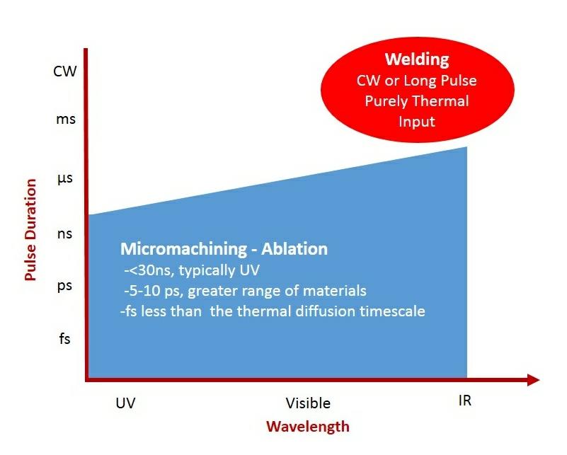
For joining and deposition, longer wavelengths and longer pulse lengths (or cw = continuous wave) are used since the purpose is to precisely deliver heat to a certain point. Longer wavelength lasers inherently introduce heat into the system by exciting the vibration-rotation bonds. Figure 1 shows a graph depicting laser wavelength plotted against pulse length. It can be seen that in the upper right hand corner the IR lasers with long pulse lengths are used for joining applications, while machining is carried out in most other quadrants. There are no big manufacturing applications currently for UV lasers with long pulse or CW output.

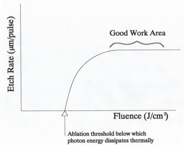
The most important thing in material removal applications is that there is strong absorption of the incident photons – at least 50 percent absorption is needed and the closer to 100 percent the better. Absorption depth is a function of the material, the incident energy density and also the laser wavelength – as a general rule, UV photons are absorbed within fractions of microns of the material surface whereas IR photons have a penetration depth on the order of 10’s of microns or more per pulse. All other things being equal, this means that UV photons are capable of higher precision and controlled ablation, but are slower than IR lasers. Figure 2 shows a representative plot of Etch rate (microns per pulse) vs. Fluence (J/cm2). Fluences below the ablation threshold show no material removal at all. Above the ablation threshold there is material removal, the rate of which increases until some point at which the curve plateaus. In general, a ‘good working area’ is on the flat part of the curve where small changes in laser output do not significantly affect per pulse material removal rates. Going higher on the curve gives no payback in removal rate, so it is generally not a good idea to do so unless other factors are involved. Note also that other factors, such as taper and HAZ (Heat Affected Zone) may also be affected by the energy density on target. It should also be noted that this absorption is intensified using shorter pulse length lasers because of non-linear effects, which in principle make an otherwise ‘transparent’ material, opaque.

Because of the wide range of available candidate lasers with differing pulse lengths, wavelengths and power outputs, almost any material can be a candidate for laser materials processing as long as the thickness and absorption are within the boundary conditions set previously. In addition, these laser tools are used in a variety of markets including medical devices (usually disposable), microelectronics, aerospace/defense, semiconductors and alternative energy.
There are many laser contract manufacturers possessing the equipment and expertise to do precision laser manufacturing, just as there are a number of systems integrators that will build a laser system for in-house production environments – some companies provide both services and systems. Contract manufacturers are an ideal resource for small runs and prototypes and can, in some cases, be more cost effective even in high volume manufacturing than large companies because of lower overhead. There is no need for a large capital expense, no equipment to maintain, and no need to hire specialized laser operators and engineers. Typically there is some recurring set up cost incurred whenever a particular job is run and there may be NRE (non-recurring engineering) if special tooling is needed. Piece pricing is dictated by the laser, complexity, number of parts per run, handling and shipping requirements. Hourly rates vary from about $100 per hour for marking jobs to $500 per hour for high power femtosecond lasers or other more ‘exotic’ laser choices.
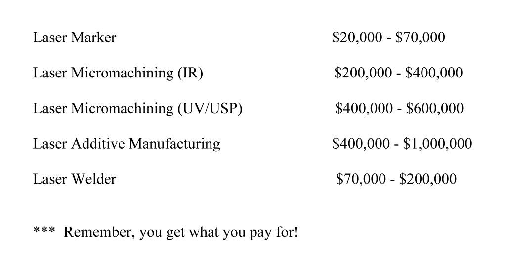
In-house systems minimize or eliminate shipping and handling issues, can be more cost effective long term, and allow onsite QC and retention of process control. This is accompanied by a large capital expense and the need to make sure that appropriate facilities and personnel are available so that the laser system works in the best manner possible. Typical system costs are shown in Table 1 and include the laser, beam delivery components, motion control elements, vision, facilities, safety/interlocks, shipping, training and documentation. A small IR marker with simple galvo and enclosure can sell for as little as $20,000 while a USP laser machining system, or a deposition system, can go for over $1,000,000.

In summary, lasers provide valuable and unique opportunities for high precision materials processing. Lasers however are just ‘fancy light bulbs’ and they need the addition of a variety of other hardware and the underlying expertise in order to make them suitable for manufacturing environments. Systems integrators can provide in-house laser solutions while contract manufacturers provide a valuable resource for prototyping, R&D and even high volume production. As parts continue to get smaller, lasers will continue to play an ever increasing role in the manufacturing of next generation products and devices.
Ronald D. Schaeffer, Ph.D. is CEO and co-founder of PhotoMachining, Inc.


