By Shiva Gadag, Radovan Kovacevic and Nilesh Ramani
Introduction:
Glass, Quartz, and Silicon are made out of sand grains consisting of Silica, SiO2. Silicon and Glass are two basic building blocks which go hand-in-hand in the fabrication of optoelectronics and microelectronics device for MEMS and Biomedical microdevice applications such as charge coupled device, lab-on-a-chip, microsensors, microfluidic arrays, PV solar cells etc.
Miniaturization of microelectronics device is the driving force for laser micromachining of transparent dielectric Glass, Quartz and semiconductor Silicon materials. The dawn of digital era has diminished the dimensions of digital devices to micron and submicron scale resulting in shrinking the size of silicon and its dioxide dielectrics based digital devices much faster than the predicted ones by the Moore’s Law. In order to meet the digital demands of the 21st century digital revolution, laser micromachining or laser lithography is the only workhorse for alternative noncontact toolless techniques for digital device micro-manufacturing. Laser micromachining with shorter pulse widths result in accurate spatial resolution, precise depth control, enhanced edge quality and minimal peripheral damage. On the other hand conventional mechanical machining of transparent dielectrics and semiconductors is economically expensive and time consuming due to the hardness and brittleness of these materials. Nano short pulses and Ultrashort pulses are most commonly used for micromachining of transparent materials. The microprocessing of hard and brittle transparent materials is accomplished due thermal ablation by heating and evaporation of surface atoms in the former laser process. The nanosecond laser micromachining can often induce some undesirable heat affected zone surrounding the feature. Whereas in the latter process, the photoablation directly results in material vaporization by breaking the atomic bond by stripping electrons. The ultrashort micromachining is cold ablation with negligible heat affected zone due to no heat transfer to surrounding area. However, ultrashort micromachining techniques are quite expensive for industrial processing of glass such as cutting, drilling and marking for touch screen glass panel displays, microfluidic chambers, solar panels and microlens and optical components for photonics industries. As a result ultrashort processing is ideal only for applications demanding extreme precisions and excellent quality with negligible HAZ. However, a similar precision and quality of micromachining of transparent, hard and brittle materials can be achieved with nanosecond short pulsed lasers but with some traces of HAZ. The nano short pulsed lasers are relatively less expensive as compared to ultrashort lasers but far more efficient than the conventional machining methods. Hence the purpose of this article is to demonstrate the ease and efficacy, pros and cons of nanoshort pulsed lasers in micromachining of transparent and brittle materials like glass and quartz using Nd: YVO4 laser harmonics.
Experimental Technique:
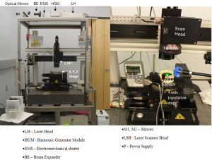
The micromachining system (Figure-1) used nanosecond pulses (11ns duration) of Nd:YVO4, DPSS, Q-switched, HIPPO laser with four harmonics generating fundamental IR λ=1064nm, 2) Green λ=532nm, 3) UV λ=355nm and 4) UV λ=266nm respectively. The micromachining gantry consisted of X,Y,Z stage with laser mounted on the top tier was focused after 8X beam expansion by

telescopic lens and 90o reflections by 2 mirrors on incoming beam opening of HurryScan-II. The scanner focused beam to diffraction limited spot diameter, d=18 microns using 100mm telecentric lens and rastered beam as per CAD feature on substrate view field of 45mm. The substrates were 1mm Corning#0215 glass and 2mm photolithographic Quartz. PerkinElmer LAMBDA UV/Vis/NIR spectrophotometer was used to determine transmittance of glass for the range of wavelengths covering four laser harmonics. Glass being transparent (T>90%) IR and green wavelengths, the first two harmonics are not suitable for micromachining. The absorbance of UV wavelengths being A>75% , the third and fourth harmonics are better suited and fourth harmonic UV λ=266nm is most ideal among the four harmonics for micromachining of glass.
Defect Diagnosis of Dielectrics:

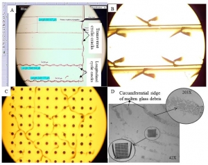
Hence UV laser was used for micromachining of glass and quartz but the initial trials with high diode current resulted in various types of defects shown in the Figure 2. Systematic analysis of the defects formed in glass during micromarking and drilling revealed two types of crack formation, namely periodic and irregular type of cracks. The primary mode-I crack formed during marking of parallel lines with high diode current at high repetition rates, propagated as cyclic crack with a well-defined wavelength of propagation all along the length of the parallel lines on glass while micromarking, The cyclic micro cracks formed by primary mode-I crack either propagate as secondary sinusoidal crack with a wavelength of propagation proportional to the wavelength of laser harmonics. Alternatively primary precracks propogate as tertiary transverse cyclic cracks along the transverse line of laser marking with a wavelength equal to perpendicular distance between the parallel lines of laser marking. The second type of periodic cracks appeared as periodic nodes of cracks at regular interval resembling tiny butterfly. The irregular type of cracks formed crack grain boundary during laser drilling of microvias on glass due very high diode currents or pulsing frequency. The irregular cracks formed colonies of cracks surrounding the microvia. The expulsion of molten glass debris often solidified as concentric circles of dendritic glass droplets surrounding the circumference of the micro vias array formed on glass.
Optimum Power, Frequency and Wavelength of Laser:
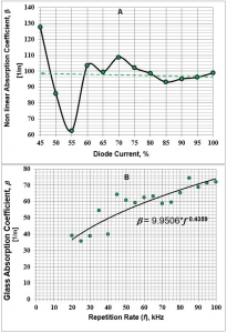
Apart from the transmittance of various wavelengths in the glass, absorbance of a suitable wavelength and its response to average power and pulsing frequency of the laser is crucial for micromachining of the glass without any defects or cracks. To establish the power and frequency response to absorbance of the laser, average power transmittance characteristics of glass for the laser harmonics were determined using the setup shown in the Figure 1. The diode current of the diode pumped solid state laser is directly proportional to average power of laser harmonics. As the diode current increased from 1 to 100% , the average power laser harmonics linearly increased to 17.5W for IR and 8.5W for Green, 5W for UV λ=355nm and 2.5W for UV λ=266nm respectively. Since absorbance characteristics of laser to diode current and frequency of pulses being identical for all four harmonics, second harmonic green laser λ=532nm was chosen to study the power and frequency response to absorption of the laser.
Intensity, I0 of power incident, P0 on glass in air, I0 = P0/(pr2) and transmitted intensity, IT of power, PT through glass IT= PT/(pr2) were measured by thermopile sensor. Applying Beer-Lambert’s law due to high optical penetration of the glass, absorption coefficient of the laser in glass thickness, l was calculated using b =-ln(IT/I0)/l . Diode current and frequency response of laser absorption in Corning glass measurement (Figure 3) indicated optimal laser power for 60-70% diode current and frequency of 55 kHz for effective micromachining.

Results:
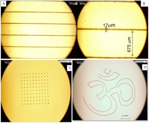
Finally using the suitable wavelength (λ=266nm) and optimal energy (5-10 µJ) and frequency (50 kHz) of 11ns short pulsed UV laser, cracks were eliminated and defects were minimized in micromachining of glass. The process optimization enabled to get fine parallel lines of 17µm and arrays of microvia of 15µm diameter at 75µm pitch, as well as etching and scribing without any cracks on glass (Figure 4). This helped to make microchannels and microfluidic tubes in 2mm thick quartz using nanosecond pulsed UV laser.

Conclusion:
An optimization of laser process parameters – wavelength, power and frequency nanosecond pulse laser crucial critical factor for micromachining of transparent dielectrics of glass and quartz with minimal HAZ, less defects and relatively free from flaws and cracks. The technical feasibility of the cost effective nanosecond pulsed lasers in microprocessing of transparent dielectrics is clearly established in this article.
Professor Radovan Kovacevic is with Dept. of Mechanical Engineering, Southern Methodist University, Dallas TX and Shiva Gadag is with ScanTech Lasers Pvt. Ltd. Nilesh Ramani is Director & CEO of Scantech Laser Pvt Ltd, India.


